Abstract: A universal dimmer scheme is proposed with modular structure. The dimmer is usable with different types of loads (in-candescent bulbs, energy saving lams, fluorescent lamps, and halogen lamps) and thus it becomes really universal. The improved topology of the power module design using MOSFETs, allows dissipating the energy stored in the reactive load (capacitive or in-ductive). This prevents the destroying of the main controlled MOSFET transistors.
1 Introduction
Generally dimmer operates as limiting the electrical power that gets to the light bulb. Nowadays there are many dimmer styles to control different types of loads. The most common electronic light dimmers operate using phase control principle. There are also some other dimmer types used in some special applications (variable transformers, simple resistors for very low power bulbs and PWM controllers for DC lights).
Proper matching of control system type to the load is very important. Using wrong dimmer type causes that the dimming does not work well, and in the worst case can damage the light dimmer and/or the lamp connected to it. Normal incandescent bulbs can be dimmed with almost any dimmer type, but some other light sources are harder to dim. Dimming can be used to extend lamp’s life in some applications where long lamp life is more important than maximum amount of generated light.
The reactive power stored in the load of the dimmer must be discharged or there will be voltage with high value on the conducting power switches (the MOSFETs). The typical incandescent bulb is an inductive load (with small value, around 5mH per 500W) as the halogen lamp is a capacitive load. The improvement of this regulator is that it can work with both of them, because of the power stage topology.
Also the use of optocoupled driver for connection with the control module allows simple galvanic insulation between the control module and the power module. The ULVO function of the driver IC allows fast and effective protection to be built.
In this article the control circuit will not be discussed and only the power module will be discussed. The reason is that the main improvement is in the power part of the dimmer.
2 Proposed universal dimmer scheme
The control module detects the zero crossing of the mains voltage and generates triangular voltage starting to rise at that point. Later a controlled reference voltage is compared to the current value of the triangular one, which creates a delay between the zero crossing and the point where the two voltages are the same. Finally a control signal is generated and sent to the galvanicaly separating MOSFET driver. This creates the appropriate signal to drive the power transistors. An over-current protection keeps the MOSFETs safe and the mains from a short circuit caused by a malfunctioned load.
2.1 Power module design
At Fig. 1 there is a simplified scheme of the power module. The most important goals to be achieved by the design are:
- stable work with different types of load
- dealing with phase delays between voltage and current without the possibility to sense this and change the control signal
- driving all MOSFETs with only one control signal
- over-current protection and short circuit protection in the power module
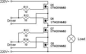
The upper MOSFET pair is functioning as an electronic switch, turning on and off the load. It will be called “serial MOSFETs”. The lower pair – “parallel MOSFETs”, use the same type of connection to a driver like the serial ones. The difference is that the parallel MOSFETs turn on with small delay (approximately 1µs) after the serial MOSFETs turn off and vice versa. This connection has some major advantages despite its higher price and increased complexity. There is no need of sensing the current offset for zero current switching and modifying the control signal. This is due to the fact that when there is no current flowing from the mains through the load it is short circuited by the parallel MOSFETs. So if the load is reactive (mainly inductive) the energy, which it returns when its supply is removed, will not destroy the serial MOSFETs. Instead it will be dissipated by the parallel MOSFETs as heat. Actually this energy is so small that the transistors will not increase their package temperature vastly and they can be used without a need of heatsink. The parallel MOSFETs are chosen to be the same as the serial ones because of their low RDSon.
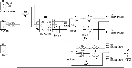
The driver block consists of two different driver circuits. The first one (Fig. 2) drives the serial MOSFETs and the second one (Fig. 3) drives the parallel MOSFETs. Optocoupled driver for connection with the control module allows simple galvanic insulation between the control module and the power module.
2.1.1 Serial MOSFET driver
The serial MOSFET driver is very simple as one can see looking at the schematic. The actual driver is the integrated circuit U1. It is HCPL3120 made by HP. This driver can directly control transistors without additional external components. It needs only one filter capacitor (C4). Its value is 100nF and it is recommended by the manufacturer. Some of the most important features of the driver are: 2A minimum peak output current; maximum supply current 5mA; supply voltage 15÷30V; under voltage lock-out protection with hysteresis; 500ns maximum switching speed.
2.1.2 Parallel MOSFET driver
The driver circuit for the parallel MOSFETs shown at figure 3 is more complicated compared to the one for the serial MOSFETs. The reason – the problems faced during the development process. The main problem is the power supply. The whole dimmer should use only one power supply. It can be single transformer with separate secondary windings and a rectifier where one needed. Most of the serially produced transformers usually have one or two galvanicaly separated secondary windings, but a transformer with three separate windings is hard to find or even impossible. Ordering a custom one will increase the price of the dimmer so this is not a good choice. The dimmer needs three power sources – one for the control circuit and two for the serial and parallel MOSFET driver circuits. A driver should be connected to MOSFET’s source and gate, but as one can see the sources of the two groups of transistors have different potentials so the driver circuits must be powered up by galvanicaly separated power supplies. To avoid the need of transformer with three secondary windings the only choice is to power up one of the driver circuits directly from the mains, using a zener diode for voltage stabilization. This raises another problem. A zener diode is not able to produce stable supply for large loads (more than 1 or 2mA of current needed for operation) while using 220V~ and the output voltage should be low (like the one needed for the driver, which is 15 volts). Having all this requirements and limits means that the driver for the parallel MOSFETs must use the mains for its power supply source and therefore it should have extremely low power consumption. The schematic at Fig. 3 is the solution. The current flowing through it during normal operation is only 10÷11μA at 15V or ≈15μW. This is achieved by using CMOS integrated circuit and only two bipolar transistors which do not consume much energy, because they drive the MOSFETs (a MOSFET is controlled by voltage but not current). A pulse transformer is used for galvanic separation between the serial and parallel channels. The signal of the control module controls the serial MOSFETs’ driver. The parallel MOSFETs’ driver uses its output so the signal becomes inverted as it is needed for correct operation.
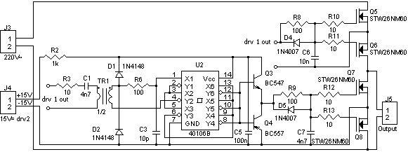
The driver consists of pulse transformer, inverter with Schmidt trigger inputs and two bipolar transistors. The transformer creates galvanic separation between the two drivers. For good output signal at the secondary winding of this transformer R-L-C circuit have to be created. At Fig. 4 there is a photograph of the realized circuit.

3 Test results
There are several tests that took place in order to confirm the idea and find out what advantages will it has in practice for the power module. The first one is heat generation test. The second one is a test of MOSFET’s driver response.
For all drawings: horizontal axis – time/div (marked as M), vertical axis – V/div
Power consumption:
- Serial channel: 2.5mA (15V supply)
- Parallel channel: 10μA (15V supply)
3.1 Heat generation
Measurements are made once using heatsink for the serial MOSFETs only (the parallel MOSFETs does not need one) and once without heatsink. The heatsink used is aluminum parallelepiped and it is not a standard grilled heat sink. Heatsink’s dimensions are as follows: 5mm thickness, 80mm width and 50mm height. Only convection is used for cooling in both cases. The measurements are made in a room with ambient temperature of 22°C. The preheating period before each measurement is 30 minutes, after which the temperature is stable and not rising. The table below shows the measured temperatures and the graphics visualize the differences in heat generation between the two cases.
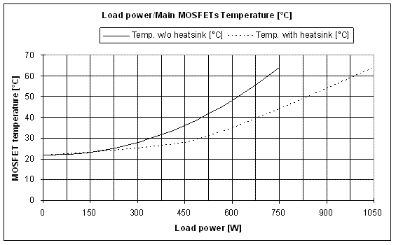
One can see that in the range up to 500 watts the serial MOSFETs does not generate too much heat and they can function properly even without using a heat sink. At 500W load the temperature reaches about 42°C, which means that if the ambient temperature rises the transistors will still be able to work without any danger of overheating. Using the mentioned heatsink the dimmer is capable of driving loads of up to more than 800W. If a large heatsink is used the maximum load can be increased beyond 1000W or more.
3.2 HCPL3120 MOSFETs driver response
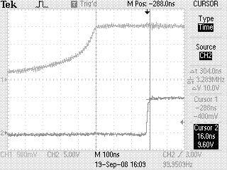
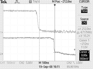
The graphics above show the response of HCPL3120 MOSFET driver to input signal. At the rising edge the delay at the output is about 300ns while at the falling edge the delay is about 210ns. This response speed is good for the dimmer requirements.
5 Conclusions
This paper proposes a universal light dimmer scheme using four MOSFET transistors. The modular structure of the dimmer makes large systems development more flexible and easy. It allows different types of control and easier maintenance. The use of optocoupled driver for connection with the control module allows simple galvanic insulation between the control module and the power module. The ULVO function of this driver allows a fast and effective protection to be built. The specific architecture of the power module makes the dimmer usable with different types of loads and thus it becomes really universal. The use of low RDS(on) Power MOSFETs makes the dimmer very efficient and it generates small amount of heat, so it doesn’t need forced cooling like heatsink. Arbitrary “on” and “off” control is possible, depending only on the control module used. A very low consumption gate drive is developed.
Acknowledgements
This article has been made with the help of: Prof. dr. ir. Alex Van den Bossche from University of Gent, Belgium (he initiated the ideas behind this project and provided help whenever it was needed); Assoc. Prof. dr. Vencislav Valchev from Technical University – Varna, Bulgaria (he is the one who made my stay in Gent possible and therefore this article would not exist without his efforts ); MSc Eng Plamen Yankov from Technical University – Varna, Bulgaria (he is the colleague who actually wrote this article based on part of my master degree thesis and also provided some help during the development of the project); MSc End Angel Marinov from Technical University – Varna, Bulgaria (he is another colleague who provided help during testing of the power module of the dimmer).
References
- Ciddor Andy – “Catching the wave: New dimmer technology comes ashore in Australia” – http://livedesignonline.com/ar/lighting_catching_wave_new/
- “Lights and electronics” – http://www.epanorama.net/links/lights.html
- Wall R. W. – “Simple Methods for Detescting Zero Crossing” – Proceedings of the 29-th Annual Conference of the IEEE Industrial Electronics Society Paper #000291
- Zilyas Malic – “Stabiele nuldoorgangsdetectie voor real-time aansturing van wermogenselektronica”
- “Power semiconductor device” – http://en.wikipedia.org/wiki/Power_semiconductor_device
- “Thyristor” – http://en.wikipedia.org/wiki/Thyristor
- “TRIAC” – http://en.wikipedia.org/wiki/TRIAC
- “Insulated-gate bipolar transistor” – http://en.wikipedia.org/wiki/IGBT
- “Power MOSFET” – http://en.wikipedia.org/wiki/Power_MOSFET
- “Insulated Gate Bipolar Transistor (IGBT) Basics” – Abdus Sattar, IXYS Corporation; IXAN0063 – http://www.ixyspower.com/images/technical_support/Application%20Notes%20By%20Topic/IGBTs/IXYS_IGBT_Basic_I.pdf
- Zaremba Don – “Using self-protected MOSFETs in ruggedized electronics” – http://www.powerdesignindia.co.in/STATIC/PDF/200807/PDIOL_2008JUL30_IND_TA_01.pdf
1 Introduction
Generally dimmer operates as limiting the electrical power that gets to the light bulb. Nowadays there are many dimmer styles to control different types of loads. The most common electronic light dimmers operate using phase control principle. There are also some other dimmer types used in some special applications (variable transformers, simple resistors for very low power bulbs and PWM controllers for DC lights).
Proper matching of control system type to the load is very important. Using wrong dimmer type causes that the dimming does not work well, and in the worst case can damage the light dimmer and/or the lamp connected to it. Normal incandescent bulbs can be dimmed with almost any dimmer type, but some other light sources are harder to dim. Dimming can be used to extend lamp life in some applications where long lamp life is more important than maximum amount of light.
The reactive power stored in the load of the dimmer must be discharged or there will be voltage with high value on the conducting power switches (the MOSFETs). The typical incandescent bulb is an inductive load (with small value, around 5mH per 500W) as the halogen lamp is a capacitive load. The improvement of this regulator is that it can work with both of them, because of the power stage topology.
Also the use of optocoupled driver for connection with the control module allows simple galvanic insulation between the control module and the power module. The ULVO function of the driver IC allows fast and effective protection to be built.
In this article the control circuit will not be discussed and only the power module will be discussed. The reason for that is that the main improvement is in the power part of the dimmer.
2 Proposed universal dimmer scheme
The control module detects the zero crossing of the mains voltage and generates triangular voltage starting to rise at that point. Later a controlled reference voltage is compared to the current value of the triangular one, which creates a delay between the zero crossing and the point where the two voltages are the same. Finally a control signal is generated and sent to the galvanicaly separating MOSFET driver. This creates the appropriate signal to drive the power transistors. An over current protection keeps the MOSFETs safe and the mains from a short circuit caused by a malfunctioned load.
2.1 Power module design
On Fig. 1 there is a simplified scheme of the power module. The most important goals to be achieved by the design are:
• stable work with different types of load
• dealing with phase delays between voltage and current without the possibility to sense this and change the control signal
• driving all MOSFETs with only one control signal
• over current protection and short circuit protection in the power module

With everything that appears to be building within this area, many of your viewpoints are generally fairly exciting. Having said that, I am sorry, because I can not give credence to your whole theory, all be it radical none the less. It looks to me that your comments are not completely rationalized and in fact you are generally your self not really wholly convinced of your assertion. In any case I did take pleasure in looking at it.
This was a project I worked on almost 15 years ago. It isn’t relevant today with LED lighthing. It did work as designed though.
very nice and working ok
Hi, good article! Could you please explain how to connect the terminals labeled as “driver 1 out” and so on. that’s why I cannot understand. thank you! regards!
I’m sorry for the late response. I see I haven’t drawn it self explanatory unfortunately. I just split the schematic so I can explain how it works without part from other blocks confusing the reader. The confusion comes from the naming of those inputs and outputs. Drv 2 In on Fig.2 has to be connected to Drv 1 Out on Fig.3. There are two groups of driver and MOSFETs for each half sine-wave. Driver 1 provides the control signal for driver 2 with a small delay so the circuit won’t short the mains power through the MOSFETs.